 Gebärdensprache
 Leichte Sprache

Winner 2020
EUV Lithography
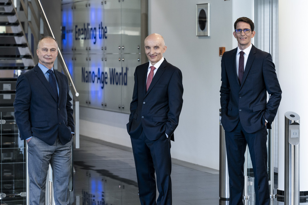
(f.l.t.r.) Dr. rer. nat. Sergiy Yulin, Dr. rer. nat. Peter Kürz, Dr. rer. nat. Michael Kösters
: weltweit die erste an Chiphersteller gelieferte EUV-Optik")
Dr. rer. nat. Peter Kürz, Dr. rer. nat. Michael Kösters and Dr. rer. nat. Sergiy Yulin have made a major contribution to developing and industrializing a technology that can be used to manufacture microelectronic components of extremely fine structures – a prerequisite for many new applications and a great step forward in the capacity of information technology (IT). Working with ASML, a supplier in the world of photolithography systems for the semiconductor industry, the three scientists and their over 2000 colleagues in development at their companies relied on a method that has been established in chip production for decades, namely optical lithography, and adapted it to use light in the extreme ultraviolet (EUV) spectral range.

Compared to standard lithography, EUV lithography is capable of producing much smaller structures, in the range of a few nanometers (a millionth of a millimeter) or about one ten thousandth of the diameter of a human hair. For this to succeed, the nominated team had to push the limits of what is technically feasible radically – which the scientists succeeded in doing with an innovative optical system and state-of-the-art laser technology.

More Details
Resume
Dr. rer. nat. Peter Kürz
- 01.05.1965
- Born in Bad Säckingen, Germany
- 1984
- Abitur at Klettgau-Gymnasium Tiengen
- 1985 - 1990
- Studies of physics at the Ludwig-Maximilians-Universität Munich, degree: Diploma
- 1990 - 1994
- Research assistant at the University of Constance
- 1990 - 1994
- Doctorate at the chair of Prof. J. Mlynek, University of Konstanz
- 1994
- Research period at the Ecole Normale Supérieure, Paris, France
- 1994 - 1996
- Scientist at NTT Basic Research Laboratories, Nippon Telegraph and Telephone Corporation, Atsugi-Shi, Japan
- 1996 - 1997
- Researcher in the central research department at ZEISS, Oberkochen
- 1998 - 1999
- Product manager at ZEISS Semiconductor Technology Segment, Oberkochen:
responsible for the development of the first 193 nm lens - 1999 - 2015
- Head of EUV Program at ZEISS Semiconductor Technology Segment, as of 2001 at the ZEISS Semiconductor Manufacturing Technology (SMT) Segment Oberkochen:
responsible for development & product launch of EUV Micro Exposure Tool, Alpha Demo Tool, Starlith® 3100 (EUV preproduction Tool), Starlith® 3300 (first EUV optics ready for mass production), Starlith® 3350 - 2015 - 2017
- Product Line Manager EUV Systems at ZEISS SMT Segment Oberkochen: responsible for development & product launch of the Starlith® 3400 (first EUV series tool)
- since 2017
- Vice President Field of Business EUV High-NA at ZEISS SMT Segment Oberkochen:
responsible for development & product launch of the next generation of EUV optics
Honors and Awards
- 2006
- Carl Zeiss Innovation Award for Leading Edge Technology for developing the optical system for the EUV Alpha Demo Tool
- 2007
- Nominated as team spokesperson for Deutscher Zukunftspreis: “Revolutionary Optics for the Computer Chip of the Future”
- 2013
- Carl Zeiss Innovation Award for Leading Edge Technology for the development of the first EUV optics suitable for series production (Starlith® 3300)
Dr. rer. nat. Michael Kösters
- 18.06.1980
- Born in Bad Hönningen, Germany
- 2000 - 2006
- Studies of physics, Rheinische Friedrich-Wilhelms-University Bonn, degree: Diploma
- 2003 - 2004
- Semester abroad in Electrical Engineering, California Institute of Technology, Pasadena, USA
- 2005 - 2010
- Research assistant, Institute of Physics, Rheinische Friedrich-Wilhelms-University Bonn
- 2006 - 2010
- Doctorate at the chair of Prof. Dr. Karsten Buse (applied optics), Institute of Physics, Rheinische Friedrich-Wilhelms-University Bonn
- 2010 - 2014
- Project manager at TRUMPF Laser- und Systemtechnik GmbH, Ditzingen:
development of a pulsed high-power CO2 laser as part of the BMBF project InProLight (Integrative process chain for resource-saving series production of lightweight components made of fibre-reinforced plastic for the automotive industry) - 2010 - 2015
- Project manager for Seed Module / EUV at TRUMPF Laser- und Systemtechnik GmbH, Ditzingen
- 2014
- Interim service manager at TRUMPF Laser- und Systemtechnik GmbH, ASML/Veldhoven, Netherlands
- since 2015
- Group lead development of High Power Seed Module / EUV at TRUMPF Lasersystems for Semiconductor Manufacturing GmbH, Ditzingen
Scholarships
- 2003 - 2004
- Scholarship of the German Academic Exchange Service (DAAD)
- 2006 - 2009
- Doctoral scholarship of Bonn-Cologne Graduate School for Physics and Astronomy
Dr. rer. nat. Sergiy Yulin
- 27.12.1965
- Born in Charkiw, Ukraine
- 1983
- Abitur at the secondary school No. 84 in Kharkiv, Ukraine
- 1983 - 1989
- Studies of physics at the Polytechnic University of Kharkiv, Ukraine, degree: diploma
- 1989 - 1999
- Research associate, Department of Metals and Semiconductors Physics at the Polytechnic University of Kharkiv, Ukraine
- 1996 - 1998
- Doctorate at the Karazin University Kharkiv, Ukraine
- 1999 - 2001
- Working contract for cooperation in various scientific projects, Fraunhofer Institute for Applied Optics and Precision Engineering IOF, Jena
- since 2001
- Research associate, Fraunhofer Institute for Applied Optics and Precision Engineering IOF, Jena
- since 2003
- Management of industrial projects for EUV lithography, Fraunhofer Institute for Applied Optics and Precision Engineering IOF, Jena
responsible for new materials for grazing incidence optics, Z-grading of EUV broadband coatings and coating of EUV optics, development of an EUV irradiation instrument, methods for protection and cleaning of EUV lithography imaging optics, development of EUV high temperature mirrors and coating of collectors of high power LPP sources - since 2003
- Training of students and doctoral candidates, Fraunhofer Institute for Applied Optics and Precision Engineering IOF, Jena
- since 2012
- Senior Principal Scientist, Fraunhofer Institute for Applied Optics and Precision Engineering IOF, Jena
Honors and Awards
- 2012
- ASML Poster Award Best Innovation: Poster „Cymer LLP collector lifetime: strategy and improvements”
- 2007
- Thuringian Research Prize: "Components and Systems for Next Generation Lithography (13.5 nm)".
Contact
Press
Frederic Franz
Communication and Implementation of Group Initiatives
ZEISS Sparte Semiconductor Manufacturing Technology
Carl Zeiss SMT GmbH
Rudolf-Eber-Straße 2
73447 Oberkochen, Deutschland
Phone: +49 (0) 7364 / 20 62 838
Mobile: +49 (0) 151 / 18 76 89 54
E-Mail: frederic.franz@zeiss.com
Web: www.zeiss.de
Spokesperson
Dr. rer. nat. Peter Kürz
Head of Field of Business High-NA EUV
ZEISS Semiconductor Manufacturing Optics
Carl Zeiss SMT GmbH
Rudolf-Eber-Straße 2
73447 Oberkochen, Germany
Phone: +49 (0) 7364 / 20 48 95
E-Mail: peter.kuerz@zeiss.com
Web: www.zeiss.de
A description provided by the institutes and companies regarding their nominated projects
EUV lithography
Entering the digital future with extreme ultraviolet light
There’s no digitalization without computing power. A smartphone today already has millions of times more computing power than the computer that accompanied the first Moon landing in 1969. This is made possible by a microchip barely the size of a fingernail that contains over ten billion transistors. New technologies and areas of application such as artificial intelligence, autonomous driving, 5G, the smart home, and Industry 4.0 need much more powerful microchips. Manufacturing these super chips requires that more and more transistors fit into an increasingly small space. Intel co-founder Gordon Moore already predicted this progressive miniaturization of electronic components in 1965. According to “Moore’s Law”, the number of transistors on a chip will double every two years – a prediction that has since become the benchmark of the semiconductor industry.
For over 40 years, optical lithography has been a key technology for manufacturing microchips. Transferring the structures of electronic components to chips is similar to projecting a slide. The projection optics images the chip structures from a mask onto a silicon wafer coated with a photoresist. This sequence is repeated about 100 times with different masks. The result is a microprocessor or a memory chip: a complex, three-dimensional electronic structure made up of transistors and circuit paths. More and more, however, this proven process is reaching its technological and economic limits. In order to achieve the computing power necessary for the ongoing global digitalization while also reducing energy consumption and production costs per chip, an entirely new approach was required.
Extreme ultraviolet light enables higher computing power
The breakthrough has now been achieved. Following over 20 years of intensive, collaborative development work, European companies and research institutes have created a revolutionary new manufacturing technology for mass-producing powerful microchips: EUV lithography. EUV stands for extreme ultraviolet, meaning light with an extremely short wavelength. This “new light” makes it possible to manufacture microchips that are much more powerful, energy-efficient, and affordable than ever before. World market leaders like Samsung and TSMC have based the production of their state-of-the-art chips on this new process since 2018. Smartphones with microchips manufactured using EUV lithography have been available on the mass market since the fall of 2019.
The transition from the laboratory to series-production is largely thanks to contributions by teams from the ZEISS Semiconductor Manufacturing Technology (SMT) segment; TRUMPF Lasersystems for Semiconductor Manufacturing; and the Fraunhofer Institute for Applied Optics and Precision Engineering (IOF). The parties involved in this development are represented by Dr. Peter Kürz, who assumed leadership of the EUV program at ZEISS SMT in 1999 and is now in charge of the development and product launch of the next generation of EUV optics; Dr. Michael Kösters, co-developer of the high-power lasers that generate the EUV light at TRUMPF; and Dr. Sergiy Yulin, who, as Senior Principal Scientist leads research projects for the coating of EUV optics at the Fraunhofer IOF.
Until now, the leading optical lithography process has relied on light sources with a wavelength of 193 nanometers. By contrast, the new manufacturing process works with only 13.5 nanometers. The resolution of the optics – and thus the dimensions of the structures on the chips – scales with the wavelength of the light used. Consequently, EUV lithography can increase transistor density by more than a factor of ten – a tremendous achievement, considering that the mere act of generating 13.5-nanometer light and harnessing it for use already pushes the boundaries of the technologically feasible.
The key is European partnerships
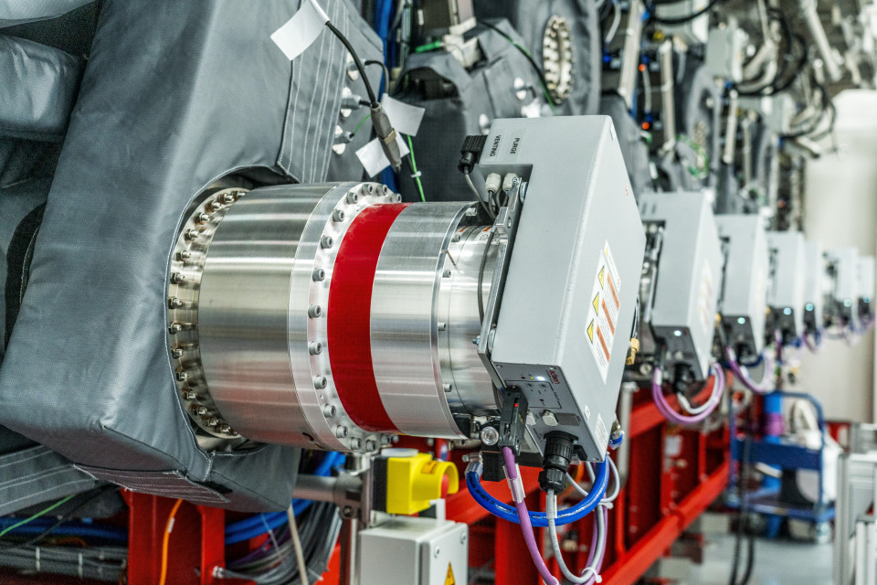
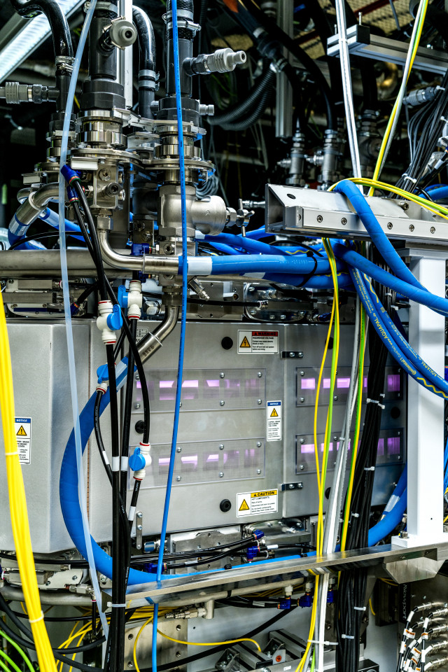
The Dutch company ASML is the world’s only manufacturer of EUV lithography machines. As an integrator, ASML designed the architecture of the complete system and the EUV source in particular. The key component in these machines is the high-power laser for the EUV light source and the optical system. And this is exactly where the semiconductor segments of laser manufacturer TRUMPF and the optics specialist ZEISS come into play.
In order to generate the EUV light, ASML and TRUMPF designed a unique light source. In a plasma source developed by ASML, 50,000 droplets of tin per second are fired into a vacuum chamber, where they are struck by two consecutive pulses from a high-power CO2 laser from TRUMPF. The “pre-pulse” hits the tin droplets, causing them to swell. The subsequent main pulse then strikes the droplets at full power. This ignites the tin plasma, which emits EUV radiation. To generate EUV light, the plasma has to be heated to a temperature of nearly 220,000 degrees Celsius – almost 40 times hotter than the average surface temperature of the sun. With 30 kilowatts of power, the TRUMPF laser required for this process is the most powerful industrial laser in the world.
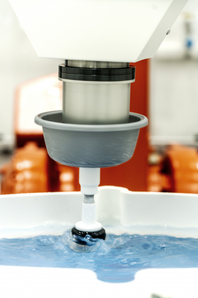
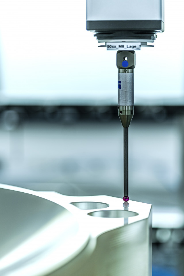
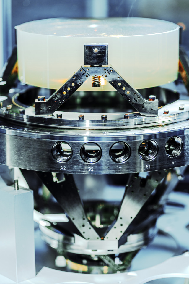
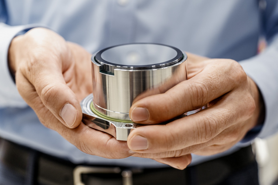
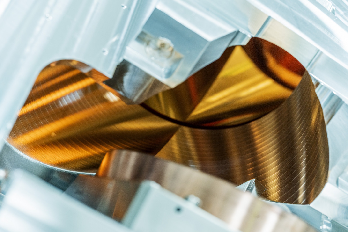
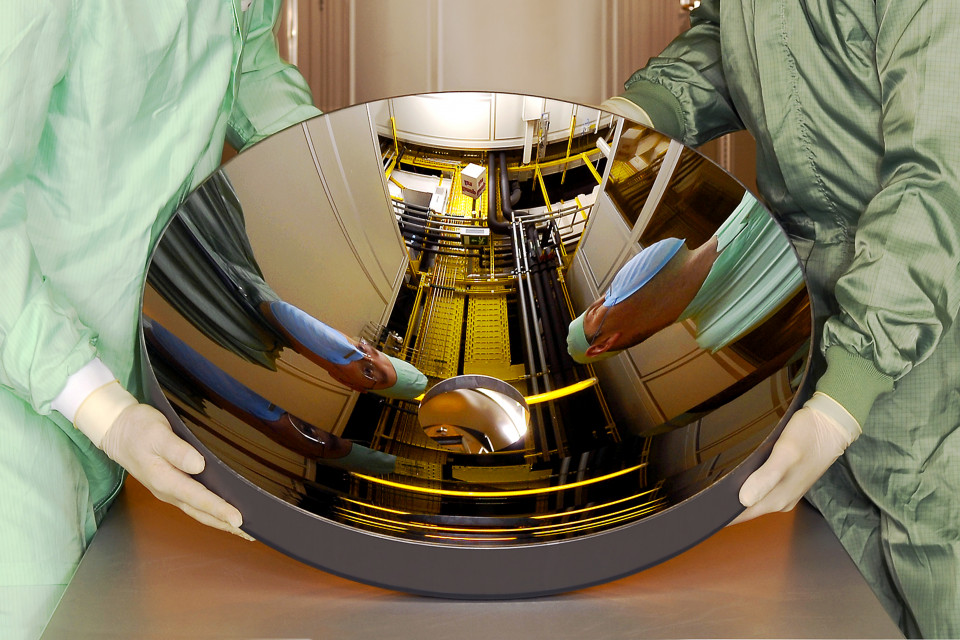
Since ultraviolet light is absorbed by all materials – including air – ZEISS SMT created an optical system for the EUV lithography machine that operates in the vacuum chamber and is made up of mirrors. Because the mirrors have to be held in position as precisely as possible during the exposure process, an entirely new mechatronics concept was required for maximum tilt stability. The results speak for themselves: If one of these EUV mirrors were to redirect a laser beam and aim it at the Moon, it would be able to hit a ping pong ball on the Moon’s surface.
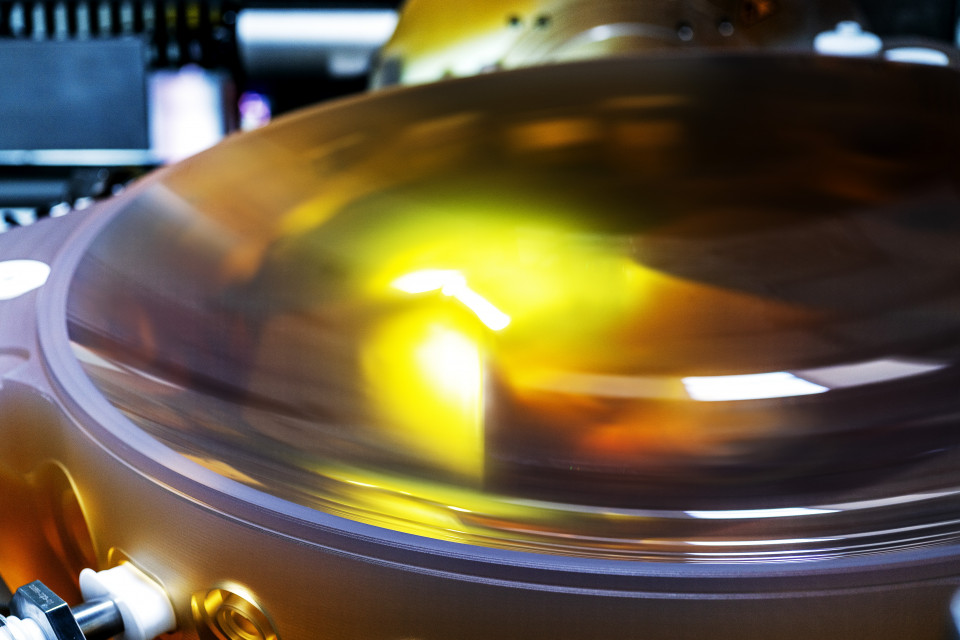
The mirrors are also the product of significant innovations. Since even the smallest irregularities cause aberrations, the world’s “most precise” mirror had to be developed for EUV lithography. If this mirror were to be enlarged to the size of Germany, the height of the Zugspitze mountain would be just 0.1 millimeters. In addition to such high precision, EUV mirrors require maximum quality and reflectivity. The Fraunhofer IOF served as an important research partner for the development of EUV mirrors through special multi-layer coatings, so-called Bragg mirrors. Here, a layer stack consisting of more than 100 layers, each one just a few nanometers thick, is applied with atomic precision. The particular challenge is achieving the highest reflexivity possible over the entire mirror surface as well as the longevity of the coating during exposure to EUV light.
The future in a new light – high tech creates jobs
In a semiconductor industry dominated by Asian and U.S. companies, EUV lithography is a European success story. The optics and light source are products of Germany’s extensive expertise in photonic technologies. Other contributing factors were a high-tech network of over 1,200 suppliers, universities, and research institutes, and the tremendous perseverance of the participating companies. From the prototype stage to readiness for mass production, the EUV source, optical system, and EUV lithography machine underwent a process that was ultimately over two decades long. Their development was supported by German and European publicly funded projects that included significant funding from the German Federal Ministry of Education and Research. The end product is a cutting-edge technology safeguarded by over 2,000 patents.
The economic significance of this technology for the semiconductor industry and for the companies involved is also tremendous. The ZEISS SMT segment began developing EUV in 1995 with just a handful of employees. Today, this has grown to over 2,000 high-tech jobs. In 2019, the annual turnover for EUV optics rose to more than 650 million euros and continues to grow dynamically. TRUMPF now has over 500 employees working in the development and production of the high-power laser, with sales of more than 400 million euros in this business area.
The future prospects are bright: ZEISS SMT, TRUMPF, and the Fraunhofer IOF are already working on the next generations of EUV optics and high-power CO2 lasers. Over the next few years, EUV technology promises to take the miniaturization of semiconductor structures to ever greater extremes and to do so cost-effectively, thus creating the basis for further technological progress and the digitalization of our everyday lives.
About ZEISS
ZEISS is an internationally leading technology enterprise operating in the fields of optics and optoelectronics. In the previous fiscal year, the ZEISS Group generated annual revenue totaling more than 6.4 billion euros in its four segments Semiconductor Manufacturing Technology, Industrial Quality & Research, Medical Technology and Consumer Markets (status: 30 September 2019).
For its customers, ZEISS develops, produces and distributes highly innovative solutions for industrial metrology and quality assurance, microscopy solutions for the life sciences and materials research, and medical technology solutions for diagnostics and treatment in ophthalmology and microsurgery. The name ZEISS is also synonymous with the world's leading lithography optics, which are used by the chip industry to manufacture semiconductor components. There is global demand for trendsetting ZEISS brand products such as eyeglass lenses, camera lenses and binoculars.
With a portfolio aligned with future growth areas like digitalization, healthcare and Smart Production and a strong brand, ZEISS is shaping the future of technology and constantly advancing the world of optics and related fields with its solutions. The company's significant, sustainable investments in research and development lay the foundation for the success and continued expansion of ZEISS' technology and market leadership.
With over 31,000 employees, ZEISS is active globally in almost 50 countries with around 60 sales and service companies, 30 production sites and 25 development sites. Founded in 1846 in Jena, the company is headquartered in Oberkochen, Germany. The Carl Zeiss Foundation, one of the largest foundations in Germany committed to the promotion of science, is the sole owner of the holding company, Carl Zeiss AG.
Further information at www.zeiss.com
About TRUMPF
TRUMPF is a high-tech company offering manufacturing solutions in the fields of machine tools and laser technology. The Company drives digital connectivity in manufacturing through consulting, platform products and software. TRUMPF is a technology and market leader in highly versatile machine tools for sheet metal processing and in the field of industrial lasers.
In 2019/20, the company employed some 14,300 people and generated sales of about 3.5 billion euros (preliminary figures). With over 70 subsidiaries, the TRUMPF Group is represented in nearly every European country as well as in North America, South America and Asia. The company has production facilities in Austria, China, the Czech Republic, France, Germany, Italy, Japan, Mexico, Poland, Switzerland, the United Kingdom and the United States.
Find out more about TRUMPF at www.trumpf.com
About Fraunhofer
The Fraunhofer-Gesellschaft, headquartered in Germany, is the world’s leading applied research organization. With its focus on developing key technologies that are vital for the future and enabling the commercial exploitation of this work by business and industry, Fraunhofer plays a central role in the innovation process. As a pioneer and catalyst for groundbreaking developments and scientific excellence, Fraunhofer helps shape society now and in the future. Founded in 1949, the Fraunhofer-Gesellschaft currently operates 74 institutes and research institutions throughout Germany. The majority of the organization’s 28,000 employees are qualified scientists and engineers, who work with an annual research budget of 2.8 billion euros. Of this sum, 2.3 billion euros is generated through contract research.
The right to nominate outstanding achievements for the Deutscher Zukunftspreis is incumbent on leading German institutions in science and industry as well as foundations.
The project "EUV Lithography - New Light for the Digital Age“ was submitted by Fraunhofer-Gesellschaft e.V..
Federal President Frank Walter Steinmeier will present the 24th German Future Prize to one of the three nominated teams on November 25, 2020.