 Gebärdensprache
 Leichte Sprache


Winner 2011
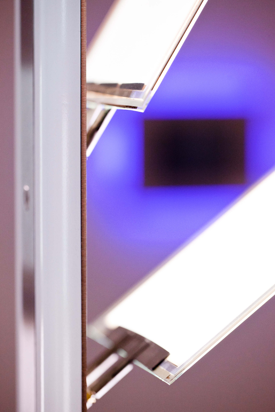
Hauchdünne Molekülschichten
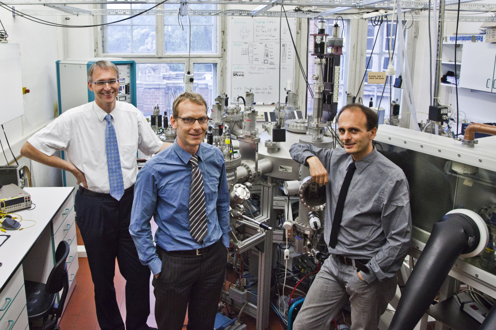
(f.l.t.r.) Prof. Dr. rer. nat. Karl Leo, Dr. rer. nat. Jan Blochwitz-Nimoth, Dr. rer. nat. Martin Pfeiffer

Prof. Karl Leo, Dr. Jan Blochwitz-Nimoth, and Dr. Martin Pfeiffer have the right materials on hand: organic semiconductors. The scientists in Dresden have succeeded in making plastics fit for use in a variety of products. They laid the foundation for innovative applications in lighting and photovoltaics which until recently were inconceivable. Karl Leo is head of the Institute for Applied Photophysics at TU Dresden and Director of the Fraunhofer Institute for Photonic Microsystems (IPMS). Jan Blochwitz-Nimoth is SCO of Novaled AG, Martin Pfeiffer is CTO at Heliatek GmbH.

The nominated scientists and their teams studied certain organic substances that have a relatively simple chemical structure. They can be used to produce transistors, light-emitting diodes or solar cells with unusual features: as thin, flexible and transparent films of almost any size. In addition, the scientists have installed the first roll-to-roll manufacturing plant in Dresden for the simple, fast and affordable production of organic light-emitting diodes (OLEDs).
more details
Resumes

Prof. Dr. rer. nat. Karl Leo
- 10.07.1960
- geboren in Freiburg i. Br.
- 1966 – 1970
- Volksschule Str. Georgen i. Schw.
- 1970 – 1979
- Gymnasium St. Georgen i. Schw.
- 1980 – 1981
- Wehrdienst: Flugzeugmechaniker
- 1980 – 1985
- Physikstudium, Albert-Ludwigs-Universität, Freiburg i. Br., Diplomarbeit am Fraunhofer-Institut für Solare Energiesysteme ISE unter Anleitung von Prof. Dr. A. Goetzberger
- 1986 – 1988
- Doktorarbeit am Max-Planck-Institut für Festkörperforschung, Stuttgart, unter Anleitung von Prof. Dr. Queisser; Promotion an der Universität Stuttgart
- 1989 – 1991
- Wissenschaftlicher Angestellter (Postdoc) bei den AT&T Bell Laboratories in Holmdel, NJ, USA, gefördert als Otto-Hahn-Stipendiat der Max-Planck-Gesellschaft
- 1991 – 1993
- Oberingenieur am Institut für Halbleitertechnik, Lehrstuhl II, Rheinisch-Westfälischen Technischen Hochschule (RWTH), Aachen (Prof. Dr. Heinrich Kurz)
- Mai 1993
- Habilitation im Fach Physik an der Rheinisch-Westfälischen Technischen Hochschule (RWTH), Aachen
- November 1993
- Professur (C4, ab 2005 W3) für Optoelektronik am Institut für Angewandte Photophysik der Technischen Universität Dresden
- 2002 – 2003
- Leiter des Bereichs „Organische Materialien und Systeme“ am Fraunhofer-Institut für Photonische Mikrosysteme, IPMS, Dresden
- seit 2004
- Stellvertretender Institutsleiter am Fraunhofer-Institut für Photonische Mikrosysteme, IPMS, Dresden
- seit 2007
- Institutsleiter am Fraunhofer-Institut für Photonische Mikrosysteme, IPMS, Dresden
Weitere Tätigkeiten:
- 2003 – 2010
- Beirat/Aufsichtsrat der Novaled AG, Dresden
- seit 2007:
- Beirat der Heliatek GmbH, Dresden
Ehrungen:
- 1989
- Otto-Hahn-Medaille der Max-Planck-Gesellschaft
- 1992
- Rudolf von Bennigsen-Förder-Preis des Landes Nordrhein-Westfalen
- 2002
- Gottfried-Wilhelm-Leibnitz-Preis der Deutschen Forschungsgemeinschaft
- 2002
- Preis der Berlin-Brandenburgischen Akademie der Wissenschaften, gestiftet von der Gottlieb-Daimler- und Carl Benz-Stiftung
- 2006
- Manfred von Ardenne Preis der Europäischen Fördergemeinschaft Dünne Schichten
- 2011
- ERC Advanced Grant funded by the 7th Framework Programme of the EU
Dr. rer. nat. Jan Blochwitz-Nimoth
- 04.12.1970
- geboren in Meißen/Sachsen
- 1977 – 1989
- Schulausbildung in Dresden, Abitur an der Spezialschule mathematisch-naturwissenschaftlich-technischer Richtung ‚Martin Andersen Nexö’ in Dresden
- 1990 – 1992
- Studium Physik an der Technischen Universität Dresden, Vordiplom
- 1992 – 1994
- Studium Physik an der Carl von Ossietzky Universität Oldenburg
- 1994 – 1996
- Studium Physik an der Technischen Universität Dresden
- 1996
- Diplomarbeit "Aufbau und Inbetriebnahme einer Anlage zur zeitaufgelösten Lumineszenzmessung mittels Summenfrequenzbildung" (Ultrakurzzeitspektroskopie an anorganischen Halbleitern).
- 1996 – 1997
- Entwickler am Ingenieurbüro Godler, Senftenberg Entwicklung und Aufbau von Projektionssystemen (Lichttechnik, Optik) für Videoprojektion im Home-Bereich.
- 1997 – 2001
- Promotionsstelle an der Technischen Universität Dresden
- 2001
- Promotion zum Thema: Herstellung und Charakterisierung organischer Leuchtdioden mit gezielter Dotierung. Diese legte die Grundlagen für Novaled.
- 20.8.2001
- Gründung der Novaled GmbH
- 2001 – 2003
- Postdoc an der TU Dresden, stellvertretender Leiter Arbeitsgruppe „organische Optoelektronik“, weitere Arbeiten an OLEDs und Vorbereitung Novaled Finanzierung
- 2003 – 2009
- Novaled GmbH und Novaled AG Technischer Leiter (CTO), Geschäftsführer (bis 2005), Mitglied des Vorstandes (ab 2006)
- 2009 – heute
- Novaled AG, Dresden Chief Scientific Officer (CSO): strategische Forschungsleitung Organische Elektronik (OLED, OPV, OTFT etc.), Projektmanagement, IP Management; Mitglied des Aufsichtsrat
Ehrungen:
- 2005
- Nominierung Deutscher Gründerpreis, Kategorie ‚Visionär’ 2005
- 2005 – 2011
- Diverse Ehrungen für Novaled (z.B. Handelsblatt 2005: das am schnellsten wachsende neue Unternehmen in Deutschland; Technology Fast50 Deutschland 2009, Clean Equity Award 2010 und andere)
Dr. rer. nat. Martin Pfeiffer
- 30.09.1967
- geboren in Aalen
- 1974 – 1978
- Volksschule in Aalen
- 1978 – 1987
- Theodor-Heuss-Gymnasium (Aalen)
- 1987 – 1988
- Wehrdienst: Morsefunker (Donauwörth)
- 1988 – 1991
- Physikstudium an der Eberhard Karls Universität Tübingen (Vordiplom 1990)
- 1991 – 1995
- Physikstudium an der Technischen Universität Dresden, Während des Hauptstudiums Förderung durch das Cusanuswerk, Bonn.
1994 Forschungsaufenthalt (4 Monate) an der Universität Lancaster (UK)
Diplomarbeit am Institut für Angewandte Photophysik (TU Dresden) unter Anleitung von Prof. Norbert Karl (Universität Stuttgart); Thema: „Energieniveaus in organischen Materialien für photovoltaische Anwendungen“
- 1995 – 2000
- Promotion am Institut für Angewandte Photophysik, Technischen Universität Dresden, unter der Betreuung von Prof. K. Leo. Graduiertenstipendium der DFG im Rahmen des Graduiertenkolleg Sensorik an der TU Dresden (1997-1999) Thema der Promotionsarbeit: „Halbleitereigenschaften dotierter organischer Farbstoffe“
- 1997
- Drei Monate Mitarbeit beim Europäischen Parlament in Brüssel: Erstellung eines Berichts zum Thema ”Erneuerbare Energien” im Namen des Ausschusses für Forschung und Technologie des EU-Parlaments
- 2000 – 2006
- Wissenschaftlicher Mitarbeiter am Institut für Angewandte Photophysik der TU Dresden.
- 2000 – 2005
- Leitung der Forschungsgruppe „Organische Optoelektronik“ (Arbeit an grundlegenden Halbleitereigenschaften dotierter organischer Schichten, OLED und Organischen Solarzellen).
- Ab 2006
- Arbeitsschwerpunkt „Ausgründung Heliatek“ und ab 1.5.2006 Leitung des Gründerförderungsprojekts „Exist Seed“ zur Gründung der Heliatek GmbH
- 2002
- Vier Monate als Gastwissenschaftler („Visiting Research Fellow“) in der Gruppe von S.R. Forrest an der Princeton University, USA. Forschungsarbeit und Veröffentlichungen auf dem Gebiet dotierter phosphoreszierender OLED
- 2003
- Mitgründung der Novaled GmbH (heute Novaled AG); bis 2006 Nebentätigkeit als wissenschaftlicher Berater der Novaled
- 6/2006
- Gründung der Heliatek GmbH zusammen mit Dr. Bert Männig, Prof. Karl Leo, Prof. Peter Bäuerle, Jens Drechsel und Dr. h. c. Harald Eggers; Einwerben einer Startfinanzierung durch den High-Tech Gründerfonds und Dr. Eggers als Business-Angel
- seit 9 /2006
- Technischer Geschäftsführer (CTO) der Heliatek GmbH
Leitung der F+E-Arbeiten
Aufbau des Teams mit Standorten in Dresden (Physik und Bauelemententwicklung) und Ulm (Chemieentwicklung)
Aufbau und vertragliche Absicherung eines Netzwerks für die Entwicklung effizienter organischer Solarzellen mit den Partnern TU Dresden, Universität Ulm, Novaled AG, Dresden, Fraunhofer Institut für Photonische Mikrosysteme, Dresden, BASF und Bosch.
Einwerben von zwei Finanzierungsrunden zusammen mit CEO Dr. Harald Eggers (2007) bzw. Dr. Andreas Rückemann (2009): Abschluss Runde A in 6/2007 (ca. 4M€; Investoren BASF, Bosch, Wellington, HTGF); Abschluss Runde B in 12/2009 (ca. 18M€; zusätzliche Investoren RWE, e-Capital, Technologie-Gründerfonds Sachsen, GP-Bullhound, weitere Investmittel von Runde A Investoren)
Schwerpunkt 2010-2012: Aufbau einer ersten Vakuum-Rolle-zu-Rolle-Fertigungsanlage für organische Solarmodule
Contact
Spokesperson
Herr Prof. Dr. rer. nat. Karl Leo
Institut für Angewandte Photophysik
Technische Universität Dresden
George-Bähr-Straße 1
(Beyer-Bau Zimmer 91)
01069 Dresden
Tel.: +49 (0) 351 / 46 33 75 33
Fax: +49 (0) 351 / 46 33 70 65
Mobil: +49 (0) 175 / 54 07 893
E-Mail: karl.leo@iapp.de
Web: www.iapp.de
Press
Kim-Astrid Magister
Pressesprecherin
TU Dresden
Pressestelle
01062 Dresden
Tel.: +49 (0) 351 / 46 33 23 98
Fax: +49 (0) 351 / 46 33 71 65
E-Mail: pressestelle@tu-dresden.de
Web: www.tu-dresden.de
Dr. Patrick Hoyer
Fraunhofer Gesellschaft
Tel.: +49 (0) 89 / 12 05 11 14
E-Mail: patrick.hoyer@zv.fraunhofer.de
Web: www.fraunhofer.de
Anke Lemke
Marketing & Communication Manager
Novaled AG
Tatzberg 49
01307 Dresden
Tel.: +49 (0) 351 / 79 65 819
Fax: +49 (0) 351 / 79 65 829
E-Mail: anke.lemke@novaled.com
Web: www.novaled.com
Steffanie Rohr
Head of Marketing
Heliatek GmbH
Treidlerstraße 3
01139 Dresden
Tel.: +49 (0) 351 / 21 30 34 508
Fax: +49 (0) 351 / 21 30 34 40
Mobil: +49 (0) 173 / 35 99 693
E-Mail: steffanie.rohr@heliatek.com
Web: www.heliatek.com
A description provided by the institutes and companies regarding their nominated projects
Imagine an entirely new type of electronic system: flexible, lightweight, unbreakable, and applied in environmentally friendly and simple processes to almost any surface as a wafer-thin layer. When these electronic devices are compared to the usual electronic systems made of inorganic semiconductors such as silicon produced in energy-intensive processes at temperatures over 1000 °C and then formed into minute crystals, the possibilities the new organic electronic systems have to offer are obvious. Conceivable applications include new types of light sources that emit a large-area, especially soft and high-quality light; innovative solar cells that can be rolled up, are exceptionally affordable and recoup the cost of the energy used in their production after a very short time. In addition, there are other new possibilities, such as integrated electronic circuits integrated in clothing, labels or bandages which can improve the quality of life and safety of numerous applications.
These innovative applications are possible thanks to organic electronics. “Organic” in this context simply means that bonds of carbon are used as they predominate in nature. Man has used these types of materials for ages, particularly as dyes. For quite some time, however, scientists have known that many of these materials also have semiconducting properties and in principle can thus assume electronic functions. However, since organic materials can also be applied to flexible substrates at room temperature, the range of possible new applications is great.
From the Fundamental Principles to Commercial Use
The most interesting aspect is that the new components attain attractive values regarding efficiency and service life: the innovative light sources, for example, with high lighting quality are of great use, but they only have a practical use if they clearly surpass the previous inefficient light sources such as the light bulb. This was the aim of the team from Dresden as they tread new paths for organic semiconductors: organic semiconductors are generally poor conductors since the materials do not contain any moving electrons. This property is a handicap to use in components such as light-emitting diodes and solar cells. The team in fundamental research at the Technical University Dresden started by addressing this problem and was inspired in their work by the findings of classic silicon semiconductor physics in which the technology of doping was developed and perfected in the 1940’s. By adding minimal amounts of other substances that produce freely moving electrons, the conductivity of semiconductors can be improved by a greater order of magnitude. This was also the approach the scientists in Dresden took in their work on organic semiconductors. In organic chemistry, however, completely different doping materials have to be used so that the premise behind Dr. Martin Pfeiffer’s dissertation was initially a search for suitable doping materials. The first experiments already revealed that the principle of doping can also be transferred to organic semiconductors. Yet the work also met with a lot of skepticism. Experts were initially condescending when they heard about the idea from Dresden: one expert from a renowned institute even stated that the components could only become worse due to doping… That was motivation enough for the team from Dresden to go on to prove that doping can considerably improve the components: they succeeded in lowering the operating voltage of organic light-emitting diodes (OLEDs) by more than a factor of two and thereby considerably improved component efficiency.
As Dr. Jan Blochwitz-Nimoth was then able to show in his thesis that highly efficient OLEDs can be produced using this method that surpass classic lighting elements such as the light bulb or even fluorescent lamps, the breakthrough of the technology was in sight. The two young scientists rapidly began pursuing the commercial implementation together with Prof. Leo by creating a spin-off from the TU Dresden and the Fraunhofer Institute for Photonic Microsystems (IPMS): this marked the birth of Novaled AG, a company that in the meantime has put this technology to work in millions of product applications: the innovative OLED displays are far superior to other solutions in contrast and color saturation, efficiency is greater due to doping, and they are easier to produce.
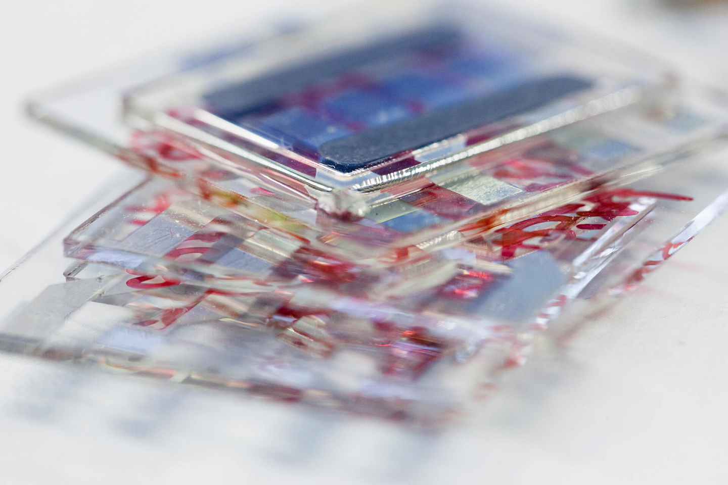
It soon became apparent that the basic doping invention can also be used in many other things: organic (OSCs) solar cells, for example, that convert incident light into electrical energy profit just as much from doping and make the designing of solar cells more efficient. Doping can be used to produce OSCs that exploit the solar spectrum much better by applying several solar cells on top of each other. With these types of solar cells containing a much improved absorber material the team in Dresden was then able to produce record-breaking efficiency and also demonstrate that these materials are extremely stable. This laid the foundation for the second spin-off, Heliatek GmbH.
The Dresden team is now devoting energy intensively to incorporating doping in other applications. They were able to demonstrate, for example, that doping can considerably improve the properties of transistors and other components with switching functions. This paves the way to a future for innovative, flexible electronics which make roll-up screens or circuitry on labels. New coating techniques were also developed for this purpose that can be used to produce components “off the roll”.
The dream of electronic systems for people that are used everywhere can thus come true. In future, it could be possible that a window is transparent during the day and provides energy as a solar cell. At night it is then used for lighting and casts the room in a pleasant soft light as if the sun were shining outside. The scientists in Dresden have thus made headway in electronics for people and invented innovative components that were not conceivable in this way in the past.
Partnership between research institutes and industry
The development of highly efficient organic components is one example of the successful cooperation between research institutes and industry: Work initially began at TU Dresden as purely basic research. It was then followed by research on actual applications at the Fraunhofer Institute for Photonic Microsystems. The industrial realization of the research took the form of spin-offs wherein the collaborators brought their developments from the university to the companies. Of the meanwhile six spin-offs that have emerged from the work at TUD and IPMS, at the top of the list Novaled AG with over 100 employees and Heliatek GmbH with over 60 employees bear mentioning. The ideal form of the transfer of know-how from research to industrial implementation was realized in these two firms: Dr. Blochwitz-Nimoth and Dr. Pfeiffer have managerial functions in the firms, and a significant number of employees from both companies moved to the firms directly after graduation to put what they learned to work.
Profile TU Dresden/Institute for Applied Photophysics
The Technical University Dresden with 36,000 students is Germany’s largest technical university. Work on organic materials has been conducted at the Institute for Applied Photophysics (IAPP) since 1985. In recent years, the institute has acquired an excellent international reputation. It constitutes the core of the “Organic Electronics Saxony (OES)” cluster which with more than 850 employees is the leading cluster in Europe in this field.
Profile Fraunhofer IPMS
The Fraunhofer Institute for Photonic Microsystems with a staff of over 200 in Dresden is devoted to the research and development of innovative optoelectronic components based on silicon and organic semiconductors. The institute cooperates on national and European projects with a vast number of industrial enterprises and institutes. Work on organic semiconductors is bundled in the COMEDD (Center for Organic Materials and Electronics Devices Dresden) at the institute. The focus of the center’s work is on scaling organic components on large substrates and developing systems based on organic components.
Profile Novaled AG
Novaled AG is a world leader in the OLED (Organic Light Emitting Diode) field and specializes in high efficiency long lifetime OLED structures and is an expert in organic electronics. The company is known for its Novaled PIN OLED® technology, its proprietary OLED materials and the customized OLED products and services. Novaled has developed long term partnerships with major OLED producers throughout the world. Based on more than 400 patents granted or pending, Novaled has a strong IP position in the field of OLED technology, and was named No. 1 in a list of ‘up and coming’ world market leaders by the German newspapers Handelsblatt and Wirtschaftswoche. Its main investors include eCAPITAL, Crédit Agricole Private Equity, TechnoStart, TechFund and CDC Innovation. For further details please visit www.novaled.com.
Profile Heliatek GmbH
Founded in 2006 as a spin-off of the Technical University of Dresden and the University of Ulm, Heliatek GmbH utilizes proprietary tandem technology to develop organic solar cells from so-called "small molecules" – organic dyes chemically synthesized from hydrocarbons. In October 2010, the Fraunhofer Institute for Solar Energy Systems (ISE) confirmed a record efficiency of 8.3% for one of Heliatek's organic solar cells. The company’s rapid progress in boosting cell efficiency, including the excellent and stable lifespan of its cells, stems mainly from the innovative organic molecules recently developed in Heliatek's laboratories. Heliatek maintains a total staff of some 65 specialists at its facilities in Dresden and Ulm and is currently building the world’s first production line for serial roll-to-roll fabrication of organic solar cells using vacuum deposition of small molecules. Production is scheduled to begin in 2012.
After financing rounds in 2007 and 2009, Heliatek has secured BASF, Bosch, and RWE as strategic investors, in addition to the pan-European venture capital company Wellington Partners and other well-known venture capital firms. Research and development work, as well as the installation of production technology, has been funded by the Free State of Saxony, the BMBF (Federal Ministry for Education & Research), the BMWi (Federal Ministry of Economics and Technology), and the European Union. More information can be found at www.heliatek.com.
The right to nominate outstanding achievements for the Deutscher Zukunftspreis is incumbent upon leading German institutions in science and industry as well as foundations.
The project “Organic Electronics – More Light and Energy from Wafer-thin Molecular Layers” was nominated by the German Research Foundation and the German National Academy of Science Leopoldina.
 Dr. rer. nat. Klaus-Dieter Rasch, Hansjörg Lerchenmüller, Dr. rer. nat. Andreas W. Bett")