Gebärdensprache
 Leichte Sprache

Nominee 2007
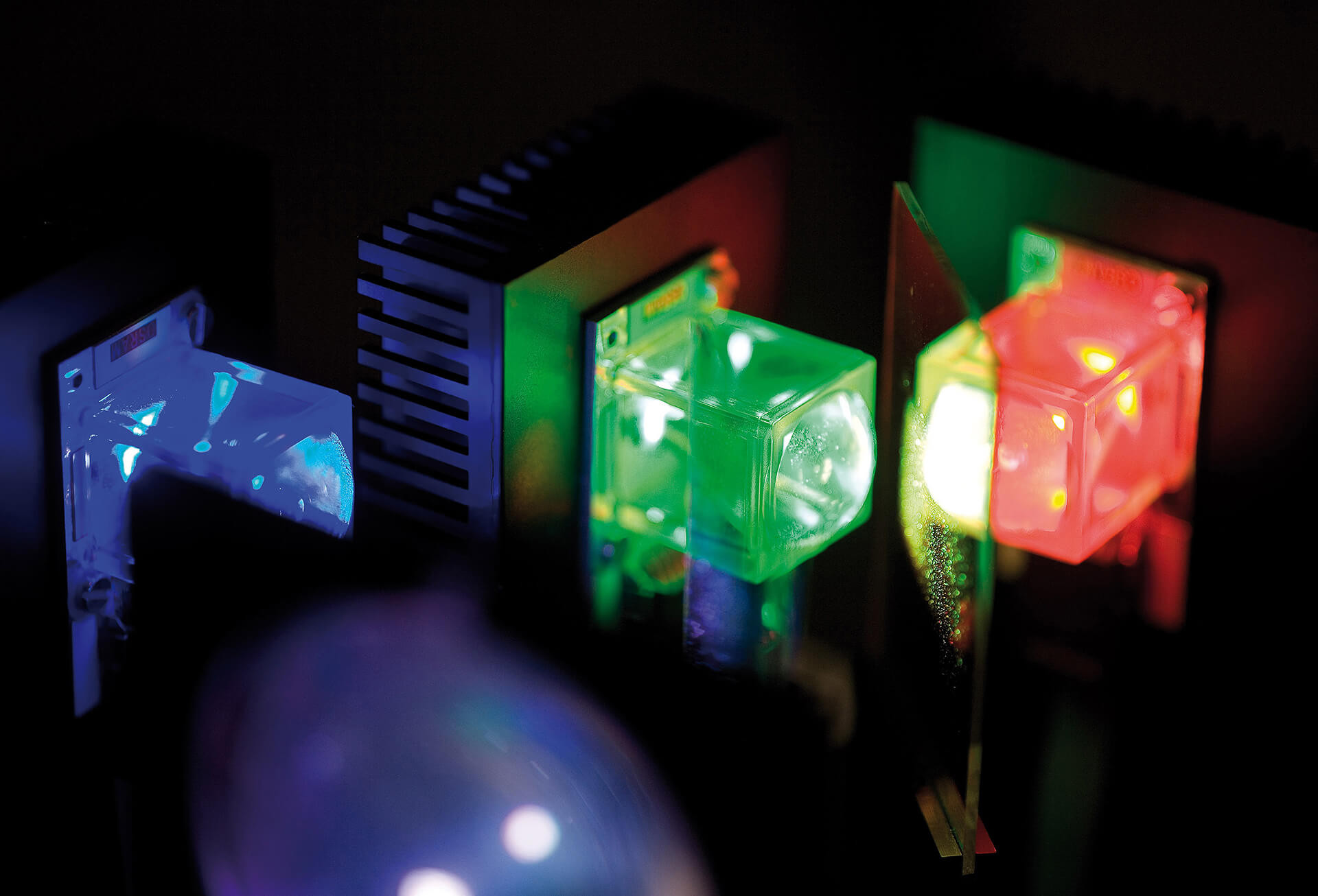
Computerchips der Zukunft
 Winfried Kaiser, Dr. rer. nat. Peter Kürz, Dr. rer. nat. Martin Lowisch")
(f.l.t.r.) Winfried Kaiser, Dr. rer. nat. Peter Kürz, Dr. rer. nat. Martin Lowisch
With a new fabrication technology for semi-conductor chips, Peter Kürz, Winfried Kaiser, and Martin Lowisch have laid the foundation for further advances in microelectronics. Peter Kürz was instrumental in this development as head of the EUV program as was Winfried Kaiser as head of product development and strategy lithography-optics, and Martin Lowisch as system engineer for EUVL systems at Carl Zeiss SMT AG in Oberkochen.
Short-wave light for precise structures
In presenting this innovation, the three nominated researchers launched a promising candidate with the potential to replace optical lithography as the method of fabricating computer chips. Used for decades in chip fabrication, optical lithography uses light focused by a sophisticated optical system to trace minute structures of processors, memory elements and conductor lines on silicon. As a rule, the shorter the wavelength of light, the smaller the structures to be created can be. Production of more powerful chips with ever finer structures was until the advent of this development only possible on systems for light with very short wavelengths.
more details
Resumes

Dr. rer. nat. Peter Kürz
- 01.05.1965
- geboren in Säckingen
- 1985 – 1990
- Studium der Physik an der Ludwig-Maximilians-Universität, München
Diplomarbeit, Thema: „Verschiedene In-situ-Präparationstechniken für die Rastertunnelmikroskopie im Ultrahochvakuum“ - 1990
- Diplom
- 1990 – 1994
- Wissenschaftlicher Mitarbeiter an der Universität Konstanz
Doktorarbeit am Lehrstuhl von Prof. J. Mlynek
Thema: „Erzeugung von Nichtklassischem Licht durch doppeltresonante Frequenzverdopplung“ - 1994
- Promotion
- 1994
- Forschungsaufenthalt an der Ecole Normale Supérieure, Paris
- 1994 – 1996
- Wissenschaftler bei den NTT Basic Research Laboratories, Nippon Telegraph and Telephone Corporation, Atsugi-Shi, Japan
- seit 1996
- Mitarbeiter der Carl Zeiss AG, Oberkochen
- 1996 – 1997
- Wissenschaftlicher Mitarbeiter in der zentralen Forschungsabteilung
- 1998 – 1999
- Produktverantwortlicher für die Entwicklung des ersten 193-nm-Objektivs
- seit 1999
- Leiter EUV-Programm: verantwortlich für die Entwicklung der EUV-Technologie bei der Carl Zeiss SMT AG
- Projektleiter Optik in der nationalen EUV-Initiative (BMBF-Projekte 13N 7867, 13 N8088 und 13 N8837) und auf europäischer Ebene (MEDEA+ Projekte EXTATIC und EAGLE, EU-Projekte EUCLIDES und More Moore)
Ehrungen:
- 2006
- Carl-Zeiss-Innovationspreis „Leading Edge“

Winfried Kaiser
- 21.07.1954
- geboren in Duisburg
- 1973 – 1982
- Studium der Physik an der Eberhard-Karl-Universität, Tübingen
- 1980 – 1982
- Diplomarbeit an der Universität Stuttgart
Thema: „Messung der optischen Übertragungsfunktion im visuellen und infraroten Spektralbereich“ - 1982
- Diplom an der Universität Stuttgart
- 1982
- Eintritt bei Carl Zeiss AG, Oberkochen
- 1982 – 1988
- Wissenschaftlicher Mitarbeiter in Optik-Design
- 1989 – 1991
- Projektleiter Optische Messtechnik
- 1992 – 1995
- Leiter Halbleiter-Entwicklungslabor
- 1995
- Leiter Produktentwicklung HL
- 1997
- Leitung Produktentwicklung und Strategie Lithographie-Optik
Entwicklung der führenden I-line- und DUV-Lithographie-Optiken, Start der 193-nm-, Immersions- und EUV-Systementwicklungen.
Initiator der EUV-Förderung in Europa und Koordinator der deutschen
EUV-Förderprojekte
Ehrungen:
- 1983
- Preis der Universität Stuttgart für besondere wissenschaftliche Leistungen
- 2003
- Carl-Zeiss-Innovationspreis „Leading Edge“
- 2004
- Carl-Zeiss-Innovationspreis “Leading Edge”
- 2006
- European SEMI Award 2006
- 2006
- Carl-Zeiss-Innovationspreis “Leading Edge”

Dr. rer. nat. Martin Lowisch
- 06.01.1967
- geboren in Berlin
- 1985
- Laborpraktikum am Zentralinstitut für Elektronenphysik, Berlin
- 1985 – 1988
- Wehrdienst
- 1988 – 1993
- Studium an der Humboldt-Universität zu Berlin
Diplomarbeit, Thema: „Sub-Picosekunden-Untersuchungen an breitlückigen
II-VI-Halbleitern“ - 1993
- Diplom
- 1994 – 1998
- Promotionsstudent und Wissenschaftlicher Mitarbeiter am Lehrstuhl
Photonik an der Humbolt-Universität zu Berlin - 1998
- Dissertation an der Mathematisch-Naturwissenschaftlichen Fakultät,
Humbolt-Universität zu Berlin
Thema: „Exzitonen in (Zn,Cd)Se- und CdSe-Quantenstrukturen – Der Übergang vom Lokalisationsplatz zum Quantenpunkt“ - 1998 – 2000
- Wissenschaftlicher Mitarbeiter an der Humboldt Universität zu Berlin
- seit 2000
- Wissenschaftlicher Mitarbeiter bei der Carl Zeiss AG
- seit 2002
- Systemingenieur für EUVL-Systeme bei der Carl Zeiss SMT AG, verantwortlich für die technische Definition und Spezifikation der optischen Systeme
- 2005
- Principal Scientist der Carl Zeiss SMT AG in den Wissensgebieten Systemdefinition und Produkt- und Technologiestrategie
Ehrungen:
- 2006
- Carl-Zeiss-Innovationspreis „Leading Edge“
Contact
Spokesperson
Dr. rer. nat. Peter Kürz
Leiter Systeme, Programm EUV
Lithography Optics Division
Carl Zeiss SMT AG
Rudoph Eberstraße 2
73447 Oberkochen
Tel.: +49 (0) 7364 / 20 48 95
Fax: +49 (0) 7364 / 20 45 09
Mobil: +49 (0) 160 / 47 92 793
E-Mail: kuerz@smt.zeiss.com
Web: www.smt.zeiss.com
Press
Dagmar Ewert
Leiterin Kommunikation und PR/
Director Marketing Communications and PR
Carl Zeiss SMT AG
Rudolf-Eber-Str. 2
73447 Oberkochen
Tel.: +49 (0) 7364 / 20 92 31
Fax: +49 (0) 7364 / 20 91 40
Mobil: +49 (0) 151 / 16 86 87 82
E-Mail: d.ewert@ smt.zeiss.com
Web: www.smt.zeiss.com
A description provided by the institutes and companies regarding their nominated projects
Decisive Breakthrough in Further Improvement in Chip Production
Progress in the electronics industry over the past 50 years has been attributable to dramatic developments in the miniaturization of electronic components and an associated reduction in function costs. As predicted by Intel’s co-founder Gordon Moore in 1965 (“Moore’s Law”), since then the number of transistors on a computer chip has doubled every two years – to over a billion transistors on a single clip today! This had laid the technological foundation for PCs in (almost) every home, cell phones, MP3 players, and the Internet’s infrastructure.
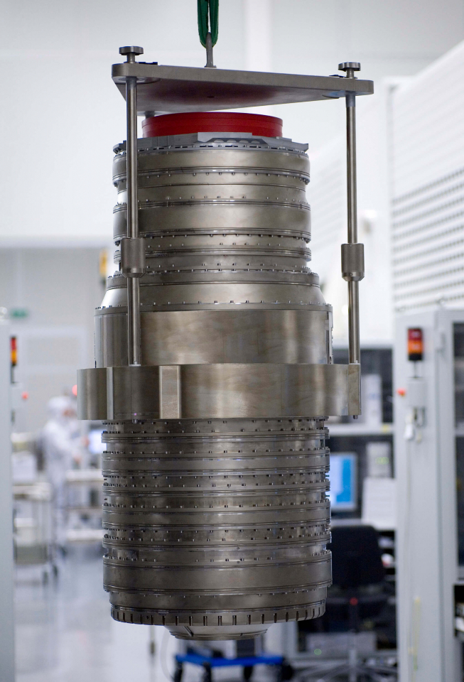
The technical challenges in the continuation of this development increase in magnitude with every new generation of computer chips. New ways must be found to realize the ever smaller structures. In December 2005, Carl Zeiss SMT, a 100% subsidiary of Carl Zeiss AG, made a breakthrough in the development of chip manufacturing technology the impact of which will be felt for the next decade. After ten years of research and development, the optical system for an EUV Alpha Demo Tool was completed and delivered to ASML B.V. (NL). ASML is a Carl Zeiss SMT partner and a manufacturer of the wafer stepper exposing machines for chip production. The Extreme UltraViolet (abbreviated as EUV) technology opens up potential for increasing the packing density of electronic components by more than a factor of 10 compared to today’s technologies.
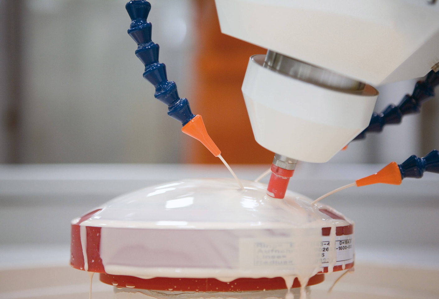
Printing Chip Structures with Light
The key to chip production is photolithography which is similar to slide projections. Chip structures are plotted on a mask. This is illuminated in the wafer stepper by means of a light source in an illuminating system and projected through the lens onto a silicon slice (the “wafer”) coated with photoresist. By developing the exposed photoresist and additional chemical processes, microstructures are produced in the wafer. This process is repeated around 40 times using various masks, whereby a three-dimensional, electronic pattern of transistors and conductors is created: a microprocessor or a memory chip.
Ultraviolet light at a wavelength of 123 nanometers (1 nanometer = 1 billionth of a meter) now makes conductors only 45 nanometers in width possible. Conventional optical lithography reaches its limits at the latest at 35 nanometers and fundamentally new technologies must be developed.
EUV Lithography – The Key to Chip Production in the Coming Decade
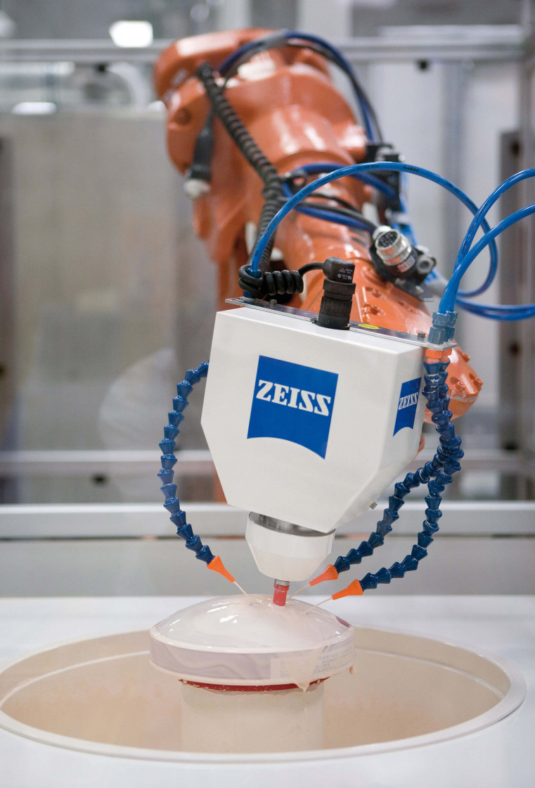
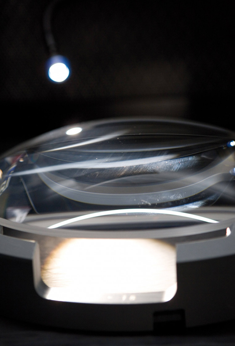
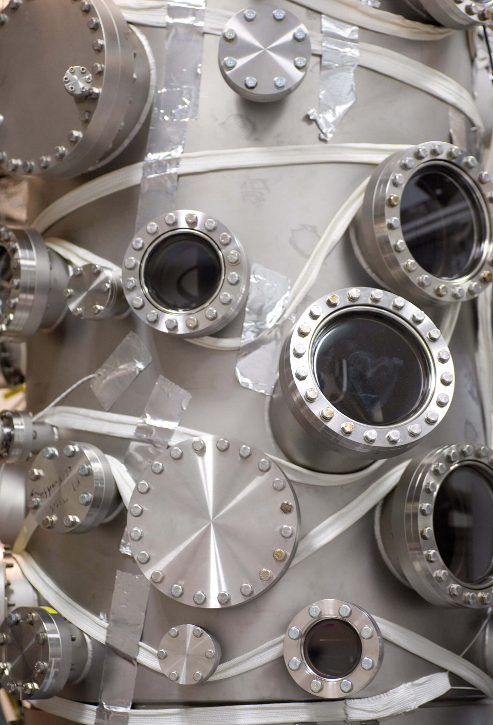
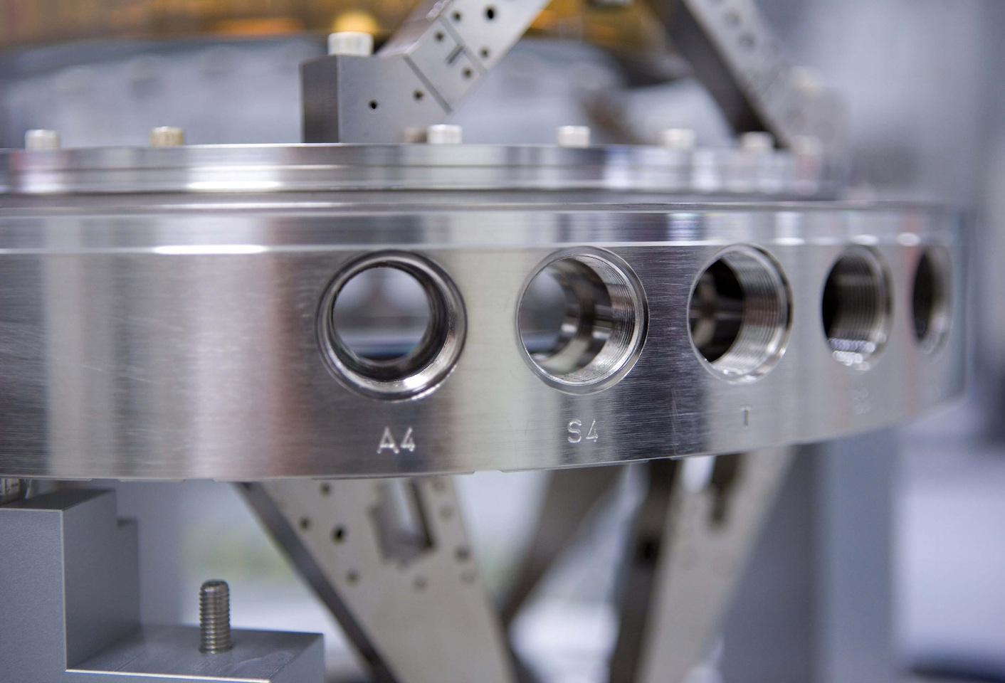
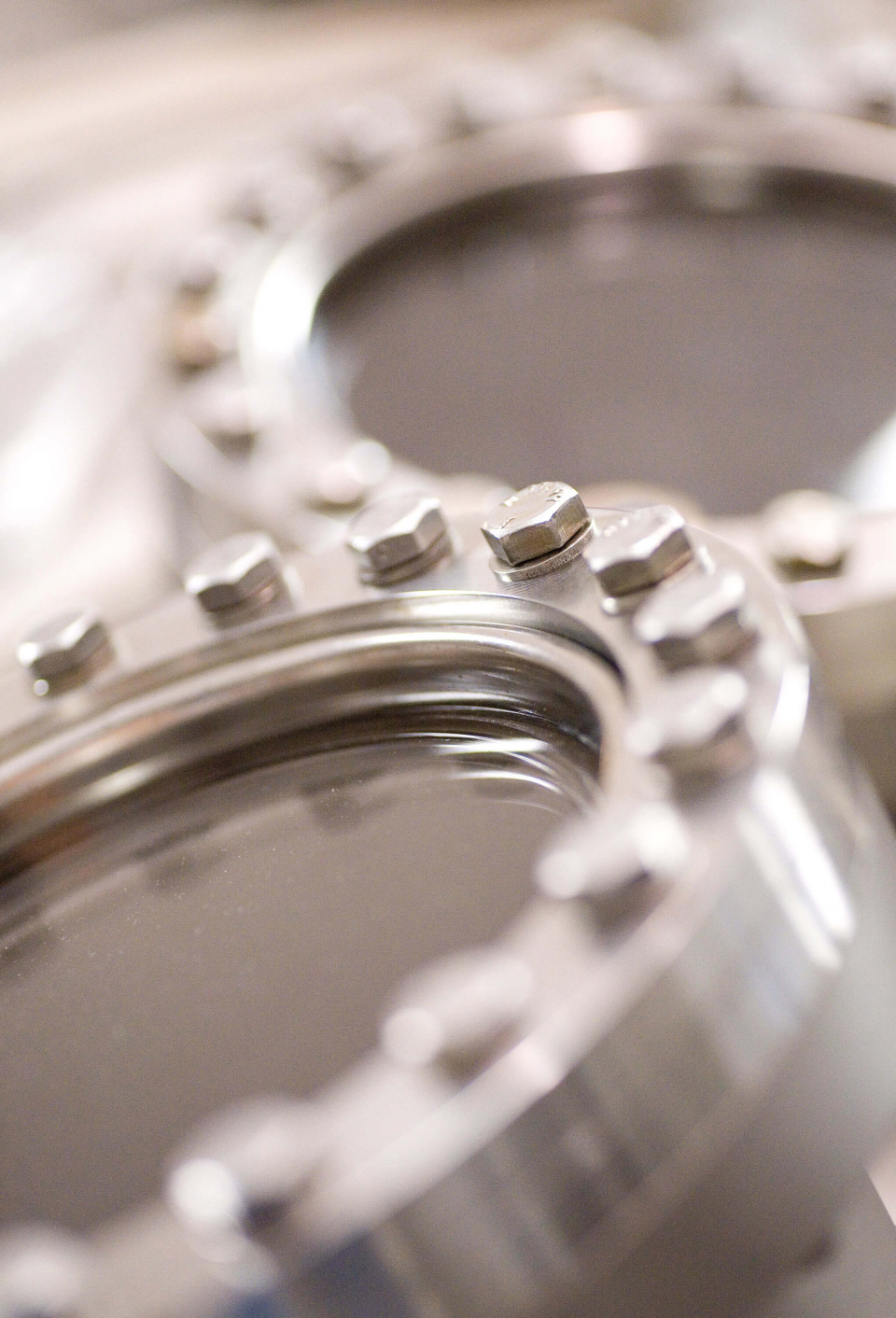
The hopes of the semiconductor industry for the next ten years are focused on EUV lithography. The technology uses light with an extremely short wavelength of only 13.5 nanometers with the potential of creating structure widths clearly less than 20 nanometers. Launching this technology, however, is associated with major challenges: no material or gas is transparent to EUV light. Compared to conventional lens-based optical lithography, the EUV optical system thus consists only of mirrors which must be operated in vacuum. Numerous top performances and world records in optical production, deposition, mechatronics, and vacuum technology have paved the way for the new technology. The mirror requirements stand out. Its surface is processed with “atomic precision”. Geometrical accuracy and surface roughness are under 0.15 nanometers. (By comparison: if the dimensions of an EUV mirror were scaled to the surface area of Germany, the highest elevations on this surface would be 1.5 millimeters at most).
With the building of the EUV Alpha Demo Tool, ASML and Zeiss have delivered fundamental proof of the feasibility of EUV lithography. In initial testing at ASML in early 2006, micro structures of 35 nanometers have been produced, thereby demonstrating the excellent imaging properties of Zeiss optics. In the meantime, lines have been shown with a width less than 30 nanometers.
The dimensions in this case are best explained in a comparison: A DIN A4 page can be printed in normal quality with a printer setting of 300 dpi (dots per inch). Each of these dots (spots) is around 85,000 nanometers in size. The Alpha Demo Tool is able to produce small spots measuring 30 nanometers. This would make it (theoretically) possible to print the entire issue of a ca. 150-page news magazine over 53,000 times on a single sheet of DIN A4 paper.
Series Use in Development
In August 2006, ASML shipped the first two EUV Alpha Demo Tools. Delivery of the machines (tool price ca. 65 million US dollars whose most valuable component is the EUV optics priced at a two-figure million Euro range) is a major milestone. Two consortiums are using the Alpha Demo Tool: one at the Belgian institute IMEC (partners include Intel, Samsung, Matsushita/Panasonic, Philips, Micron, STMicroelectronics, Texas Instruments, TSMC, and Qimonda) and one at the American research center Albany NanoTech (partners are IBM, Qimonda, Micron, AMD, Sony and Toshiba). The chip manufacturers use these tools for their process development based on EUV lithography that paves the way to industrial applications. The technology is expected to establish itself rapidly since, compared to all alternatives, it will allow for high-productivity chip manufacturing and, because of its similarity to production techniques used today, it is easily introduced to chip production facilities. ASML already has firm orders from chip manufacturers for the follow-up device to Alpha Demo Tools.
The process forms the basis for tapping into an enormous market over the next decade: demand worldwide is forecast at more than 100 EUV systems per year, amounting to a market volume of over one billion Euros for the EUV optics. Even more important is the influence on the entire semiconductor industry (annual sales currently more than 200 billion Euros) whose technological process and growth is guaranteed for numerous years by the EUV technology.
High-technology creates Jobs
Together with partner ASML of the Netherlands, Carl Zeiss SMT has advanced over the past decade to become a global market leader in the area of optical lithography. In the mid 1990s, Carl Zeiss SMT increased sales more than tenfold from 80 million Euros to 860 million Euros. At the same time, the number of employees similarly rose meanwhile to around 2,400. Moreover, in the Swabian mountains, the world’s most state-of-the-art factory for lithography optics has been built. The EUV technology secures existing high-tech jobs and promotes further growth in the coming decade.
The ten-year development period of the new EUV optics entailed considerable investment: over 100 million Euros went into work at Carl Zeiss SMT. Major technological steps forward were made within the scope of EU development projects and of the German Federal Ministry for Education and Research.
With the building of the EUV Alpha Demo Tool that is currently without equal worldwide, ASML and Carl Zeiss SMT have reinforced their position as technology leaders and gained a considerable development edge over Japanese competitors who will not complete comparable systems before the end of 2007. This leading position is secured by more than 50 patent applications (more than 20 patents have already been granted).
The EUV technology at Carl Zeiss SMT was developed through the years by a team of more than 100 scientists and engineers. Major contributions were also made by a network of cooperation partners. Specific mention must be made of the radiometry lab of the Physikalisch-Technischen Bundesanstalt at the BESSY-2-Synchrotron in Berlin, the Fraunhofer Institute IWS in Dresden, the Johannes Heidenhain company in Traunreuth, the Institutes FOM Rijnhuizen and TNO Delft in the Netherlands, as well as the companies ASML and Philips.
Three individuals have been nominated to represent these teams for the German Future Prize. Winfried Kaiser initiated EUV development in the mid-1990s and promoted it in Germany and throughout Europe, laying the foundation for its worldwide acceptance. Dr. Peter Kürz hads headed the EUV program at Carl Zeiss SMT since 1999; he is responsible for development and manufacturing of the EUV optics. Dr. Martin Lowisch, as system engineer, is responsible for the technical design of the optical system and coordinating system specifications with ASML and clients.
The right to nominate candidates for the German Future Prize (Deutscher Zukunftspreis) is granted to leading German institutes in science and industry, as well as foundations.
The project “Revolutionary Optics for Production of the Computer Chip of the Future” was nominated by the Federation of German Industries (BDI, Bundesverband der Deutschen Industrie e.V).