 Gebärdensprache
 Leichte Sprache


Nominee 2013
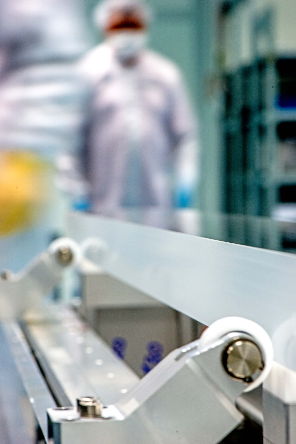
Kristalline Schaltschichten
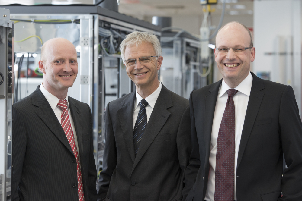
(f.l.t.r.) Dr. rer. nat. Ralph Delmdahl, Dipl.-Ing. Rainer Pätzel, Dr.-Ing. Kai Schmidt

Dipl.-Ing. Rainer Pätzel, D. rer. nat. Ralph Delmdahl und Dr.-Ing. Kai Schmidt found the solution. They have developed an innovative laser system capable of producing large-area backplanes made of crystalline silicon on glass - the basis for manufacturing high-quality smart phone displays whose appeal lies in their excellent resolution. Rainer Pätzel is head of marketing at Coherent, a laser technology company based in Göttingen, Ralph Delmdahl works for the company as product marketing manager, Kai Schmidt is the director of the Research & Development division.

Demand for smart phones continues to grow. In three years, it is assumed that two billion people worldwide - twice as many as today - will own one of these multi-talented devices that combines a cell phone and portable mini-computer. The success of the small-sized high-tech devices is primarily based on their large touch-screen displays that allow easy handling and display of high-resolution pictures, animations and video clips. The only requirement is a pixel density of at least 250 dpi: the display's individual pixels are so close together that they cannot be seen by the human eye. With the pixels the underlying electronic circuits also have to be shrunk to minute dimensions. This can only be achieved by using thin layers of polysilicon - a material consisting of numerous small silicon crystals and produced by selectively melting amorphous silicon onto a glass substrate.


more details
Resumes

Dipl.-Ing. Rainer Pätzel
- 28.07.55
- geboren in Ostercappeln
- 1974
- Fachabitur, Osnabrück
- 1977 - 1981
- Studium, Biomedizinische Technik, Fachhochschule Gießen
- 1981
- Diplom-Ingenieur für Biomedizinische Technik
- 1981 – 1993
- Leiter des Kundendienstes für Lasersysteme Lambda Physik, Göttingen
- 1993 – 2001
- Produktmanager, Laser in der DUV-Lithographie, Lambda Physik, Göttingen
- 2001 – 2003
- Entwicklungsleiter - Schmalbandige Excimerlaser für die DUV-Lithographie, Lambda Physik, Göttingen
- Seit 2003
- Marketingleiter, Laser und Optische Systeme Coherent LaserSystems GmbH & Co KG, Göttingen
Ehrungen:
- 1994
- Innovationspreis der Deutschen Wirtschaft „Metall-Keramik-Laserröhre“
- 2010
- Berthold Leibinger Innovationspreis
- 2012
- Innovation Award Laser Technology
Dr. rer. nat. Ralph Delmdahl
- 31.07.1966
- Geboren in Berlin
- 1986
- Abitur in Offenbach am Main
- 1986 – 1988
- Wehrdienst in Germersheim und Burbach
- 1988
- Beginn Chemie-Studium, Johann Wolfgang Goethe-Universität Frankfurt am Main
- 1994
- Chemie-Diplom, Johann Wolfgang Goethe-Universität Frankfurt am Main
- 1994 – 1996
- Wissenschaftlicher Mitarbeiter, Institut für Physikalische und Theoretische Chemie, Johann Wolfgang Goethe-Universität Frankfurt am Main
- 1996
- Beginn Studium der Wirtschaftswissenschaften, FernUniversität in Hagen
- 1996 – 1998
- Wissenschaftlicher Mitarbeiter, Institut für Physikalische und Theoretische Chemie, Technische Universität Braunschweig
- 1998
- Promotion in Chemie bei Prof. Dr. K.-H. Gericke, Technische Universität Braunschweig
- 1999 – 2000
- Post-Doc, Department of Molecular and Laser Physics, Institute for Molecules and Materials, Radboud Universität Nijmegen, Niederlande
- 2000 – 2005
- Produktmanager für Excimerlaser und Farbstofflaser, Lambda Physik AG, Göttingen
- Seit 2005
- Product Marketing Manager für Excimerlaser und Optiksysteme, Coherent LaserSystems GmbH & Co. KG, Göttingen
- 2006
- Abschluss als Diplom-Kaufmann und Diplom-Volkswirt, FernUniversität in Hagen
Ehrungen:
- 2002
- Commendation for Excellence in Technical Communications
- 2010
- Berthold Leibinger Innovationspreis
- 2012
- Innovation Award Laser Technology
Dr.-Ing. Kai Schmidt
- 02.09.1965
- geboren in Suhl
- 1984
- Abitur, EOS Meiningen
- 1984 – 1986
- Grundwehrdienst
- 1986 – 1991
- Studium Physik, Schwerpunkt Festkörperphysik an der Humboldt Universität zu Berlin
- 1991
- Graduierung zum Diplom-Physiker an der Humboldt-Universität zu Berlin
- 1991 – 1992
- Wissenschaftlicher Mitarbeiter am Institut für Theoretische Elektrotechnik der Technischen Universität Berlin
- 1992 – 1994
- Wissenschaftlicher Mitarbeiter am Kernforschungszentrum CERN, Genf
- 1994 – 1998
- Wissenschaftlicher Mitarbeiter am Institut für Bioprozess- und Analysenmesstechnik e.V., Heiligenstadt
- 1998 – 2000
- Projektleiter Forschungszentrum für Medizintechnik und Biotechnologie e.V., Bad Langensalza
- 2000
- Promotion zum Dr.-Ing. an der Universität der Bundeswehr in München
- 2000 – 2005
- Projekt- und Gruppenleiter Lithografielaser, Lambda Physik AG, Göttingen
- Seit 2006
- Forschungs- und Entwicklungsleiter für Excimerlaser und Optiksysteme, Coherent LaserSolutions GmbH & Co. KG, Göttingen
Ehrungen:
- 2010
- Berthold Leibinger Innovationspreis
- 2012
- Innovation Award Laser Technology
Contact
Spokesperson
Dipl.-Ing. Rainer Pätzel
Coherent LaserSystems GmbH & Co. KG
Hans-Böckler-Straße 12
37079 Göttingen
Tel.: +49 (0) 551 / 69 38 155
E-Mail: rainer.paetzel@coherent.com
Press
Dr. Ralph Delmdahl
Coherent LaserSystems GmbH & Co. KG
Hans-Böckler-Straße 12
37079 Göttingen
Tel.: +49 (0) 551 / 69 38 397
E-Mail: ralph.delmdahl@coherent.com
www.Coherent.de
www.Coherent.com
A description provided by the institutes and companies regarding their nominated projects
Crystalline backplanes for vivid displays - bye, bye pixels!
A new generation of systems for excimer laser annealing is the basis for mass manufacturing fast and energy-saving backplanes which render mobile displays the high-resolution, all-rounders that have become a self-evident part of present-day reality.
Mobile displays have in just a few years revolutionized our information society and our communication behavior. Mobile internet access has become the basis of our communication culture. Now, in the era of digital media, users can directly access the collective knowledge of mankind – anytime and anywhere. The visual perception of digitized information content occurs primarily via digital mobile displays.
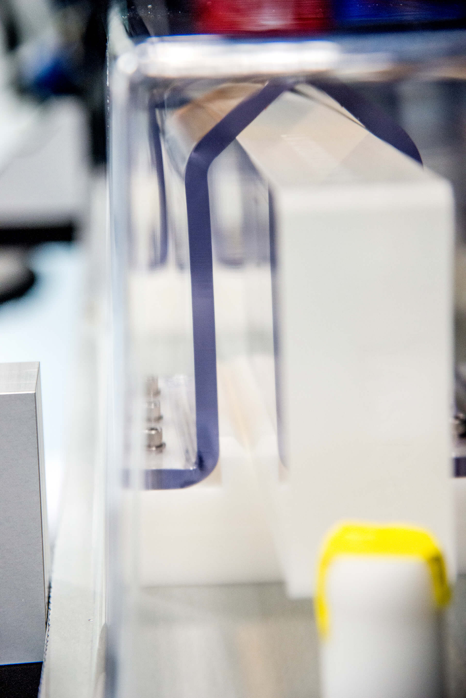
Digital displays are composed of individual pixels – arranged in a similar manner as the squares on a squared paper. The more pixels, the more information can be displayed on a screen. The current benchmark for mobile displays is a pixel density, at which it is impossible for the naked eye to see individual pixels. This is the case for pixel densities above and beyond 250 pixel per inch (ppi). The general trend towards increasing pixel densities can only be complied with shrinking dimensions of the pixels and their thin-film transistors (TFTs). The realization of the essential electronic circuits can be achieved only on the basis of highly conductive polysilicon layers usually applied on glass carriers. Crystalline switches are smaller than conventional switches made of amorphous silicon, i.e. they absorb less light and hence save energy by reducing the power consumption for backlighting. Furthermore, crystalline backplanes switch pixels much faster, which is why higher display refresh rates for video content are achieved.
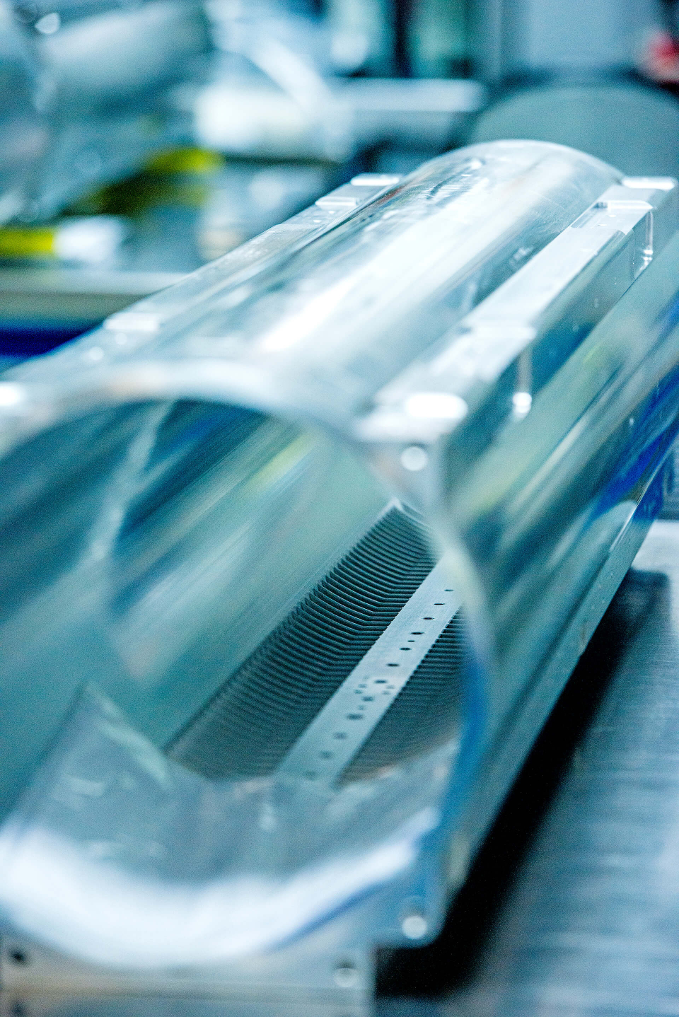
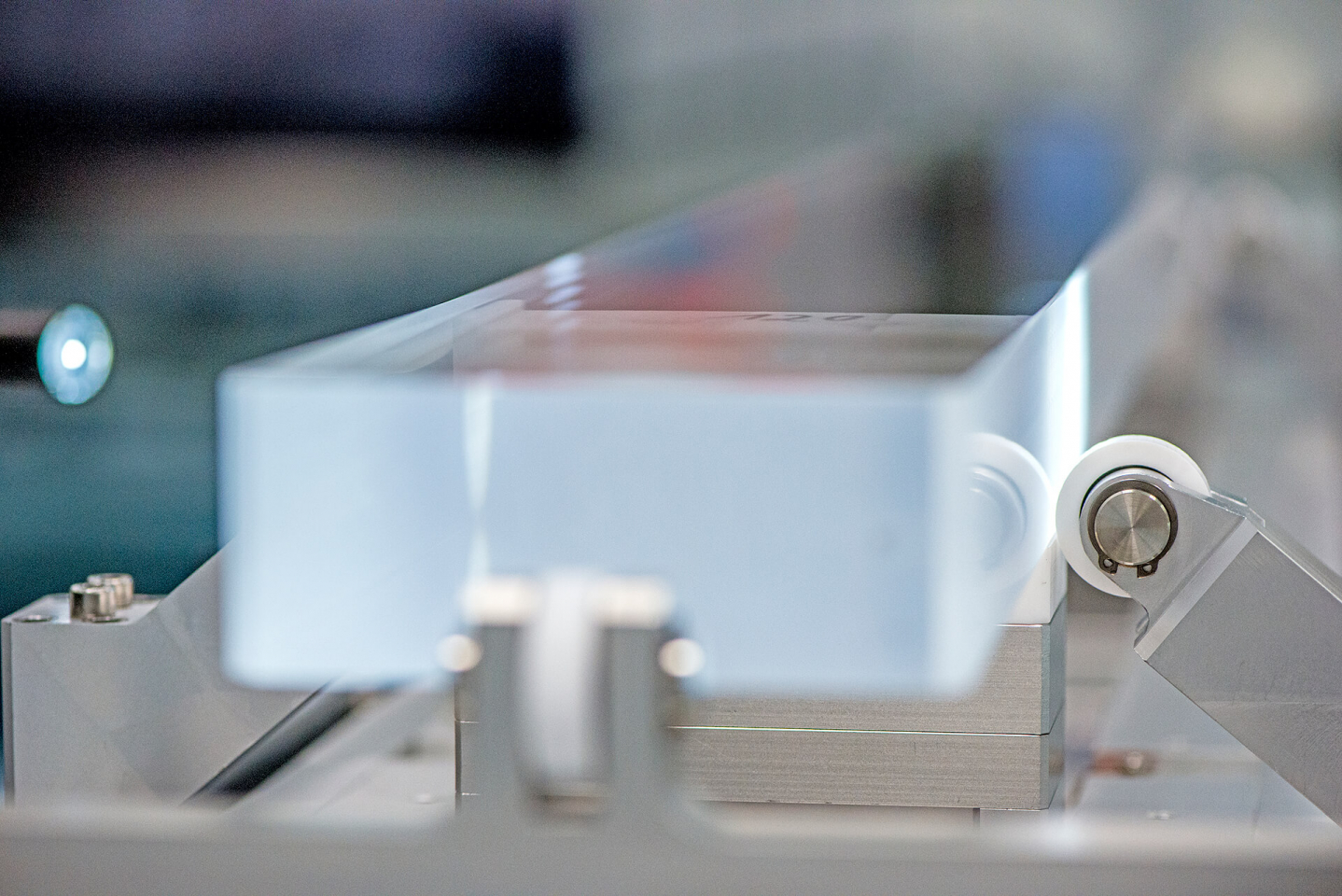
The worldwide number of smartphone users will expand over the next 3 years from the present 1 billion to 2 billion. The demand for polysilicon is driven by the rapidly increasing market penetration of high-resolution LCD and OLED displays. The leap in demand for polysilicon is met by the worldwide unique excimer laser annealing system „VYPER/LineBeam750“. It is able to generate the extremely thin crystal layer – 2,000 times thinner than a human hair – by the meter via selectively melting an amorphous silicon film. Thanks to the short UV wavelength of 308 nm and the short laser pulse duration of several nanoseconds, the energy of the laser light is concentrated on the silicon layer and is not directed to the heat-sensitive glass substrate below. The „VYPER/LineBeam750“ system currently represents the sole production potential for mass manufacturing of the crystalline key material being the salient feature in the high-resolution mobile displays of all manufacturers. The formula is simple: Without the „VYPER/LineBeam750“ system, no crystalline display backplanes for high-resolution mobile devices.
Extremely thin crystalline layers on glass substrates about the size of a king size bed.
Until spring 2011, the excimer laser annealing method was limited to glass substrates of size 90 cm x 70 cm, from which individual displays were cut. The limiting factors were the achievable laser power and the length of the line beam which is scanning the substrate in the process. Yet, some 0.6 square meter size substrates were way too small for meeting the since 2010 steeply rising demand for polysilicon layers triggered by the trend towards increasing pixel densities. Doubling the line beam length as well as the laser power became indispensable, in order to realize crystalline layers extending on some 2.8 square meter size substrates (1500 mm x 1850 mm). The nominated scientists and their teams have come up with a solution that enabled the doubling of the performance parameters required by the market. In a first step, a time synchronization of the ultraviolet light pulses of two specially developed high power laser oscillators accurate to within 5 nanoseconds could be achieved through the development of the patented “EquiSwitch” technology. The 1.2 kilowatt „VYPER“-laser thus created formed the basis for a second challenge: An optical design managing more than one oscillator beam. To this end, for the first time, the „LineBeam750“ beam delivery system was designed. It integrates, blends and homogenizes two separately supplied excimer laser beams and projects the resulting line-shaped beam - 75 cm long and thin as the stroke of a sharp pencil - onto the substrate. The resulting „VYPER/Line Beam“ concept allows for the addition of more oscillators, thus providing further scalability potential. This is particularly useful for manufacturing crystalline layers for OLED-TVs on gigantic 5.5 square meter size substrates (3 m x 2.8 m). In this way, for instance, up to six OLED-TVs with a screen size of 55 inch can be obtained per polysilicon substrate. The first systems with a power level of 2.4 kilowatt and correspondingly larger line beam length have meanwhile been delivered.
By introducing „VYPER/LineBeam750“, the nominated team succeeded in turning excimer laser annealing being the only viable production method of fabricating polysilicon layers from a niche activity into large scale production. Rainer Pätzel is Head of Marketing at Coherent LaserSystems GmbH & Co. KG. Ralph Delmdahl oversees the product marketing activities of the excimer laser manufacturer. Kai Schmidt is Head of the Research and Development department in Göttingen.
Monthly production capacity: 15,000 square meters of polysilicon for some 2 million mobile displays
The continuous demand for „VYPER/LineBeam750“ systems for the production of polysilicon panels has resulted in an almost doubling of the employment at the Göttingen site since its launch in early 2011. By now, more than 50 systems are working in display mass production. The throughput of a „VYPER/LineBeam750“ is approximately 15,000 square meters of polysilicon per month - an area as big as two football pitches. Converted in 4 inch display equivalents this is a production of more than 2 million displays a month.
The market for polysilicon-based displays will continue to grow strongly over the next years. The demand for „VYPER/Line Beam“ systems needed to fabricate the essential crystalline layers is currently driven primarily by the soaring smartphone segment. This impetus is reinforced by the steadily growing share of high-resolution mobile displays featuring pixel densities beyond 250 ppi. A trend which has since reached the larger tablet displays and which is poised to trigger the next wave of demand.
Market researchers expect the slim OLED-TVs will in the long-run outperform LCD-TVs owing to their fast response time, good color rendering and high contrast. It is expected that 70 million OLED-TVs will be sold in 2020 with display sizes of 45 inch and larger commanding a market share of two thirds. As OLED displays fundamentally require crystalline backplanes even at low pixel densities, it is safe to assume a large polysilicon demand from the OLED-TV segment in the future. With the „VYPER/LineBeam“ system, the nominated team has brought into being the future-oriented production infrastructure for polysilicon being the basis for upcoming growth markets in the digital age that built upon it.
Coherent LaserSystems GmbH & Co. KG
The Göttingen company Coherent LaserSystems GmbH & Co. KG is the world leader and pioneer in the development and production of excimer lasers and beam delivery systems for ultraviolet laser applications in research, medicine and microelectronics. More than 15,000 lasers and optical systems have been shipped during the past 40 years, including the world’s first excimer laser annealing system for the display industry - 15 years ago. Today, the VYPER/LineBeam systems are developed, marketed and built on-site by 350 employees in Göttingen with access to a network of both national and international suppliers.
Further information at www.coherent.com
The right to nominate outstanding achievements for the Deutscher Zukunftspreis is incumbent upon leading German institutions in science and industry as well as foundations.
The project “Crystalline backplanes for vivid displays - bye, bye pixels!” was nominated by DIHK – The Association of German Chambers of Commerce and Industry.
