Gebärdensprache
 Leichte Sprache

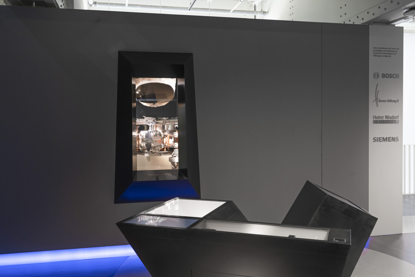
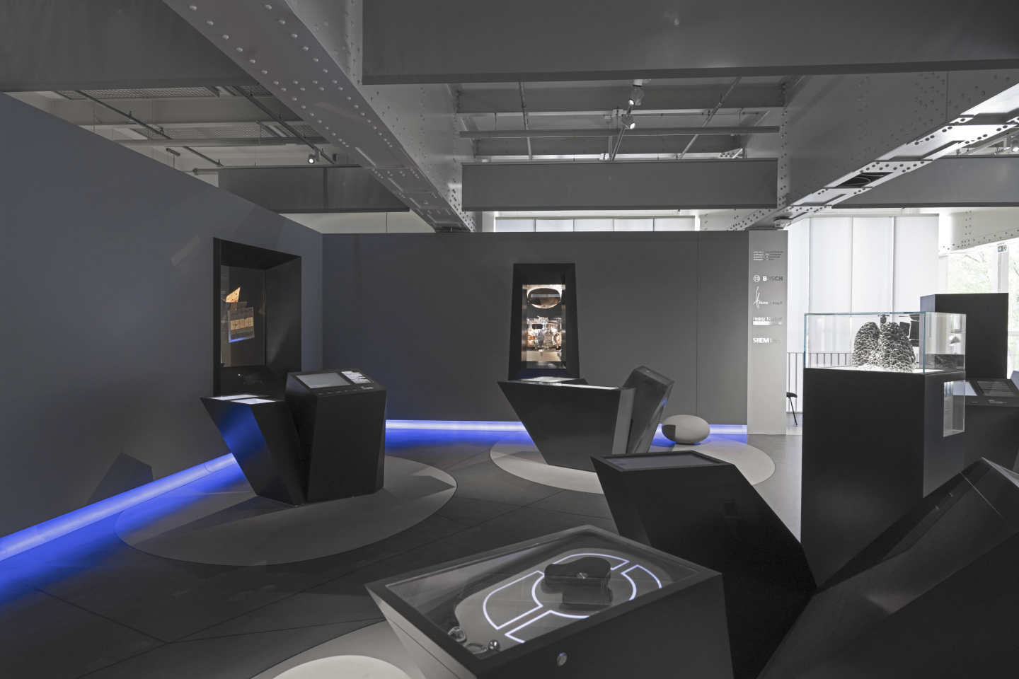
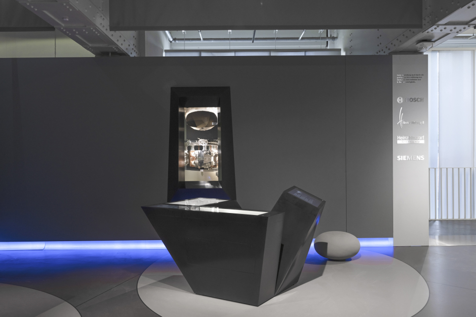
Exhibition design
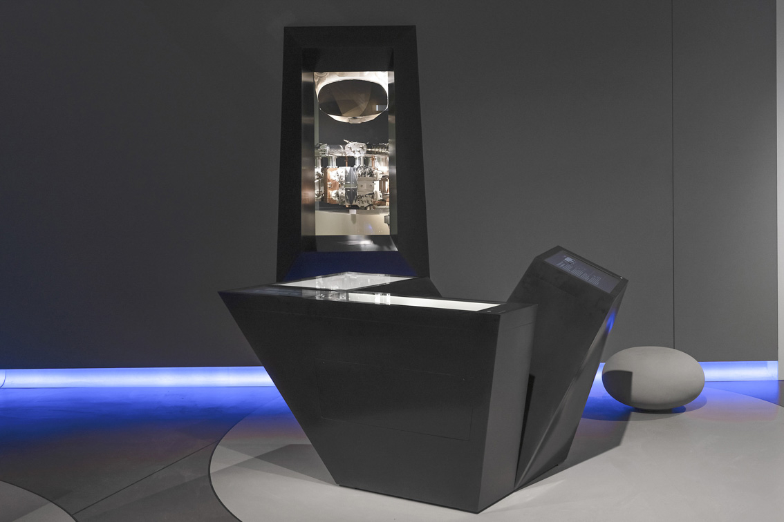
The module of the winners 2020
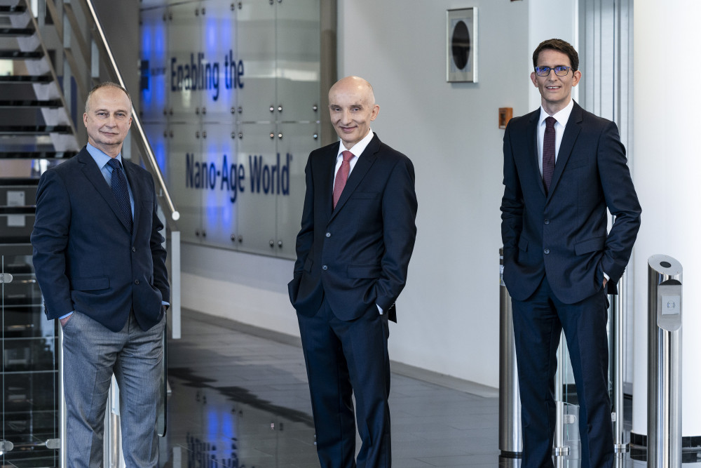
(f.l.t.r.) Dr. rer. nat. Sergiy Yulin, Dr. rer. nat. Peter Kürz, Dr. rer. nat. Michael Kösters

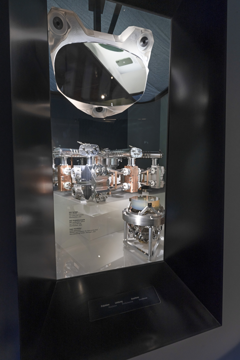
With their development, they have dramatically pushed the borders of what has been technically feasible, including a novel optical system and laser technology at the heart of the new system for EUV chip production. Their innovation made a major contribution to the manufacturing of microelectronic components of extremely fine structures. In 1965, Gordon Moore, one of the co-founders of Intel, postulated that “the number of transistors on a chip will double every two years”. “Moore’s Law” continues to apply even today, not least of all thanks to EUV lithography.

In the module itself, the complex process of EUV lithography is explained in detail based on different components, seen here also in smaller exhibits. With an interactive exhibit, visitors learn how important a mirror’s coating is for its function. Statements by the three prizewinners, located in the module’s media terminal, explain how long and complex the development process was and how their joint efforts were crowned with success.